Description
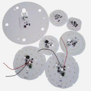
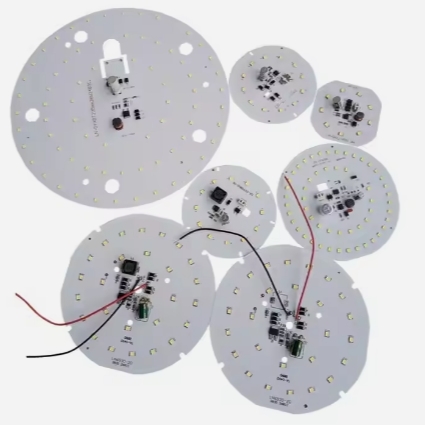
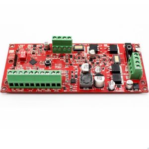
Aluminium core pcb assembly led pcba solutions
Structure Of Aluminum PCBs
Aluminum PCBs are aluminum based CCLs (CCL is a type of base material of PCBs). AluminumPCBs are actually quite similar to FR4 PCBs. The basic structure of Aluminum PCBs is four layered. It consists of a layer of copper foil, a dielectric layer, an aluminum base layer and aluminum base membrane.
General Design Guidelines for Aluminum PCBs
Thermal Considerations:
Aluminum PCBs are often used in high-power applications, so it’s important to consider thermal management in your design. Make sure to include thermal vias to help dissipate heat and avoid hot spots.

Trace Width and Spacing:
When designing aluminum PCBs, it’s important to consider the width and spacing of your traces. The wider the trace, the better the current carrying capacity. However, wider traces also take up more space on the board. Make sure to balance the need for current carrying capacity with the available board space.

Copper Thickness:
The thickness of the copper layer on an aluminum PCB is typically thinner than on a traditional FR4 PCB. This is because aluminum has better thermal conductivity, so less copper is needed to dissipate heat. Make sure to select a copper thickness that is appropriate for your application.

Mounting Holes:
Aluminum PCBs are often used in applications where they need to be mounted to a heatsink or chassis. Make sure to include mounting holes in your design that are appropriately sized and spaced.

Solder Mask:
The solder mask on an aluminum PCB should be designed to withstand high temperatures. Make sure to select a solder mask that is appropriate for your application.

Plating:
Aluminum PCBs are typically plated with a thin layer of nickel and gold to protect the copper traces from oxidation. Make sure to select a plating thickness that is appropriate for your application.

PCB Layout:
When designing an aluminum PCB, it’s important to consider the overall layout of the board. Make sure to leave enough space between components to allow for proper heat dissipation, and avoid placing components in areas that are likely to generate hot spots.

Step 1: Preparing Aluminum PCB Laminates
For single-sided one-layer aluminum PCBs, the first step of aluminum PCB manufacturing is preparing and pre-treating the laminates. This step is done automatically on automated guide vehicles. This is because we need to prevent scratches that result from carrying laminates.

Step 2: Generating Circuits on the Copper Layer
We place a film drawing the circuit image above the copper layer that is covered by photoresist liquid. Under the UV light, the photoresist under the circuit image hardens and forms a protective film. While photoresist in the rest areas is still liquid and is washed away. Then we use sodium hydroxide to etch away exposed copper.

Step 3: Drilling Positioning Holes on Production Panels
On aluminum PCBs, positioning holes are designed for screw connection with other parts and the product shell. As the manufacturer, we also need to design positioning holes on technology edges for punching and routing. We pouch out positioning holes on the production panels using a punch press.

Step 4: Solder Mask Printing
Solder mask printing on aluminum PCBs has no differences from other PCBs. Under the UV light, the solder mask ink gets dry in the exposure-development method. Then the panels are baked in an oven to let the solder mask cure. Since aluminum PCBs are mainly used for lighting, the solder mask color is usually white. Many customers choose 85% light reflective white solder masks.

Step 5: Silkscreen Printing
Silkscreens are the text and symbols printed on the solder mask to mark the components, polarity, quality standards, and the company logo. PCB ink is pressed and printed on the circuit boards through a stencil with openings.

Step 6: Surface Finish
At this step, the exposed copper PCB pads are sprayed, immersed, or plated with an antioxidant and solderable film, which is called the surface finish. The surface finishes on aluminum PCBs include ENIG, OSP, lead-free HASL, immersion tin, immersion silver, and immersion gold.

Step 7: Punching and Routing Aluminum PCBs
Here we come to the last manufacturing step, punching and routing. Usually, aluminum PCB punching and routing are completed on the same machine so we include them as one step.
About Our Company:
Shenzhen Thriver Digital Technology Co.,Ltd focas on PCB&PCBA Manufacturer for over 10 years.
Our best solution service :
A,One Stop Service For PCB PCBA Design, PCB Layout Design, PCB PCBA Manufacture;
B,Components Purchasing, PCB PCBA Assembly, Testing, packing and Shipping;
C,Copy PCBA, PCB PCBA Reverse Engineering.
